The History we have made so far.
Books
Chapter 8: Microscopy of defects
in semiconductors
F. Tuomisto (Ed.): Characterisation and Control of Defects in Semiconductors (IET, London, 2019)
ISBN-13: 978-1-78561-655-6
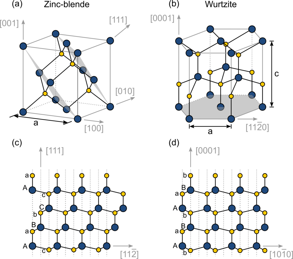
Piezoelectric III-V and II-VI Semiconductors
Massabuau and Calahorra, Reference Module in Materials Science and Materials Engineering (Elsevier, 2020)
ISBN: 9780128035818
2026
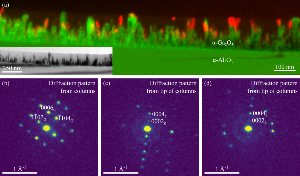
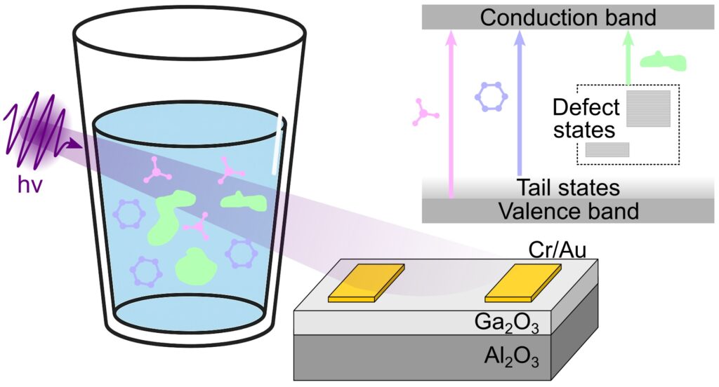
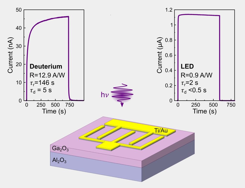
Gallium oxide-based photodetectors for water quality monitoring
Nicol et al., ACS Applied Optical Materials XX, XXX (2026)
DOI: 10.1021/acsaom.5c00620
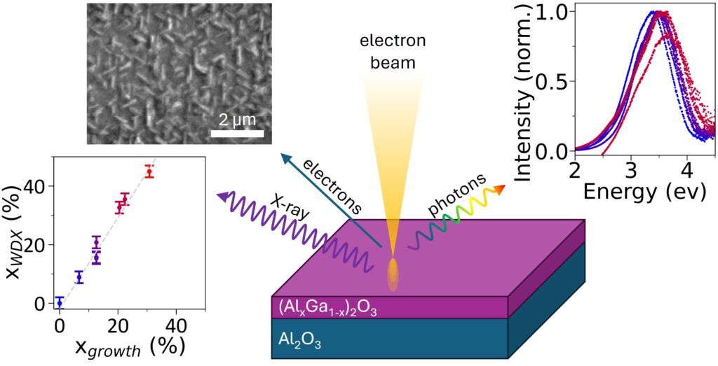
Microanalysis of β-(AlxGa1−x)2O3 Films Grown by MOCVD
Maruzane et al., Materials 19, 672 (2026)
DOI: 10.3390/ma19040672
2025
Consistent reporting of performances in Ga2O3 UV-C photodetectors
Nicol et al., APL Electron. Devices 1, 026108 (2025)
DOI: 10.1063/5.0255413
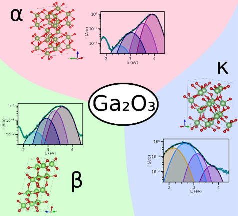
Comparative Study of the Optical Properties of α-, β-, and κ-Ga2O3
Penman et al., Phys. Status Solidi B 262, 2400615 (2025)
DOI: 10.1002/pssb.202400615
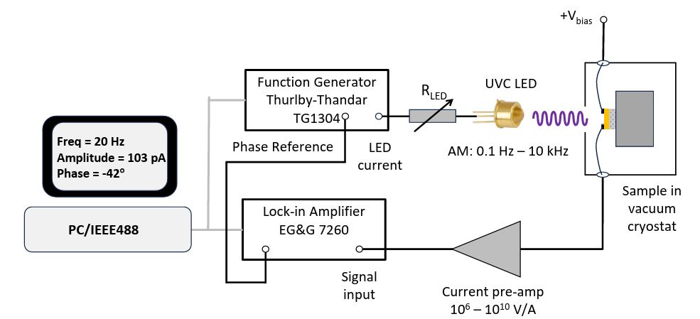
Carrier transport and electronic defects in gallium oxide studied by photoconductivity techniques
Reynolds et al., J. Phys.: Conf. Series 2952, 012001 (2025)
DOI: 10.1088/1742-6596/2952/1/012001
Luminescence properties of dislocations in α-Ga2O3
Maruzane et al., J. Phys. D: Appl. Phys. 58, 03LT02 (2025)
DOI: 10.1088/1361-6463/ad8894

Data-driven microstructural optimization of Ag-Bi-I perovskite-inspired materials
Nandishwara et al., npj Computational Materials 11, 2010 (2025)
DOI: 10.1038/s41524-025-01701-7
Stark manifold ultraviolet emission in Gd-implanted beta-Ga2O3 thin films
Williams et al., Mat. Phys. Today 54, 101731(2025)
DOI: 10.1016/j.mtphys.2025.101731
Effect of oxygen content on p-type electrical conductivity in β-Ga2O3 films
Park et al., Mat. Sci. Semi. Proc. 200, 110003(2025)
DOI: 10.1016/j.mssp.2025.110003

2024
Atomic scale observation of threading dislocations in α-Ga2O3
Mullen et al., AIP Advances 14, 115018 (2024)
DOI: 10.1063/5.0235005
Constant photocurrent method to probe the sub-bandgap absorption in wide bandgap semiconductor films: the case of α-Ga2O3
Nicol et al., physica status solidi (b) 261, 202300470 (2024)
DOI: 10.1002/pssb.202300470
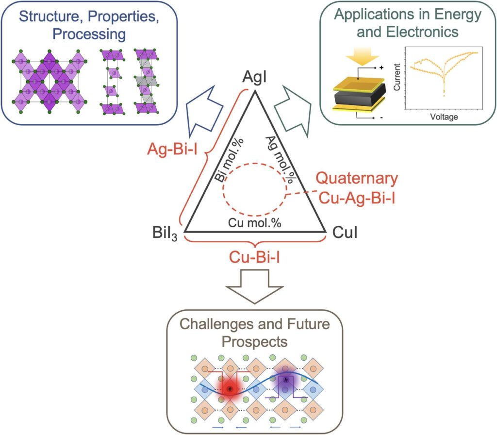
Progress and applications of (Cu–)Ag–Bi–I semiconductors, and their derivatives, as next-generation lead-free materials for photovoltaics, detectors and memristors
Zhu et al., International Materials Reviews 69, 19 (2024)
DOI: 10.1177/09506608231213065
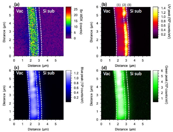
Tin gallium oxide epilayers on different substrates: optical and compositional analysis
Hunter et al., physica status solidi (b) 261, 2400137 (2024)
DOI: 10.1002/pssb.202400137
Sub-surface imaging of porous GaN distributed Bragg reflectors via backscattered electrons
Sarkar et al., Microscopy and Microanalysis 30, 208 (2024)
DOI: 10.1093/mam/ozae028
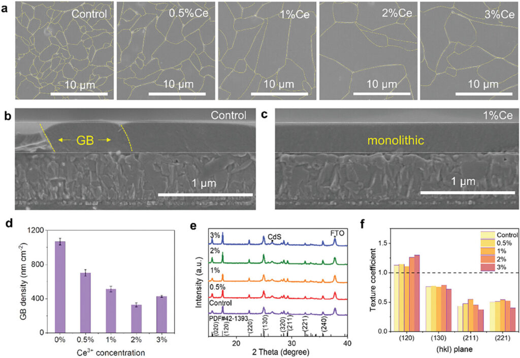
Grain Engineering of Sb2S3 Thin Films to Enable Efficient Planar Solar Cells with High Open-Circuit Voltage
Liu et al., Adv. Mater. 36, 2305841 (2024)
DOI: 10.1002/adma.202305841
2023
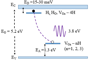
Hydrogen-related 3.8 eV UV luminescence in α-Ga2O3
Nicol et al., Appl. Phys. Lett. 122, 062102 (2023)
DOI: 10.1063/5.0135103
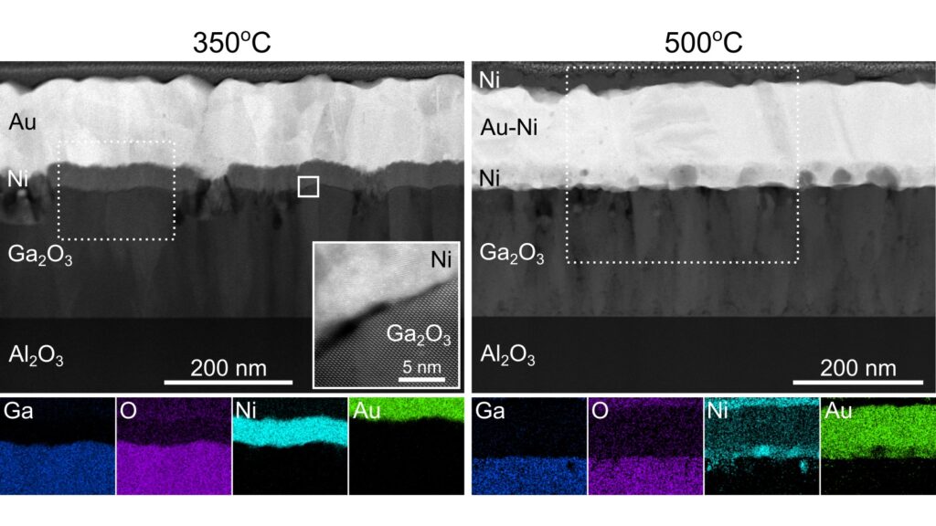
Ni/Au contacts to corundum α-Ga2O3
Massabuau et al., Jap. J. Appl. Phys. 62, SF1008 (2023)
DOI: 10.35848/1347-4065/acbc28
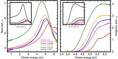
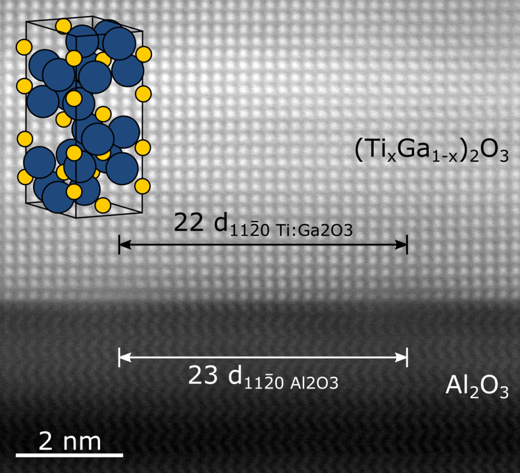
Redshift and amplitude increase in the dielectric function of corundum-like α-(TixGa1-x)2O3
Kluth et al., Appl. Phys. Lett. 122, 092101 (2023)
DOI: 10.1063/5.0139725
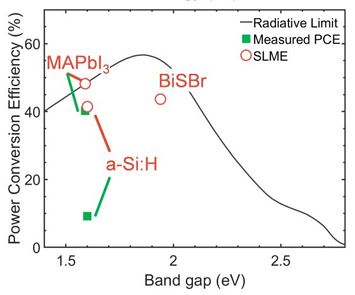
Air-Stable Bismuth Sulfobromide (BiSBr) Visible-Light Absorbers: Optoelectronic Properties and Potential for Energy Harvesting
Guo et al., J. Mater. Chem. A 11, 22775 (2023)
DOI: 10.1039/D3TA04491B
2022
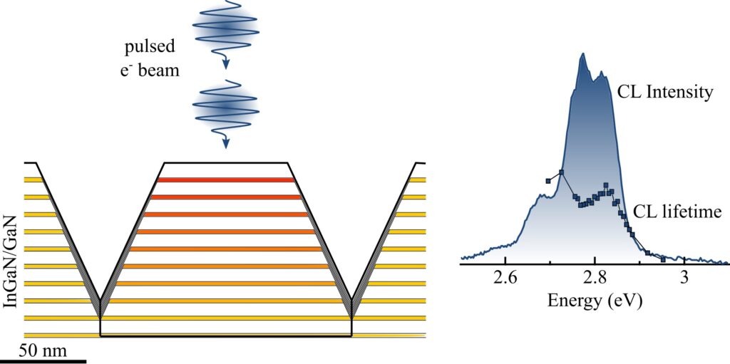
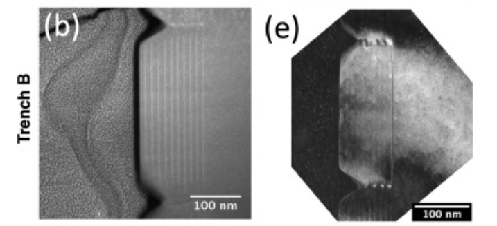
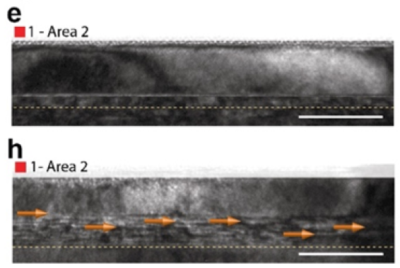
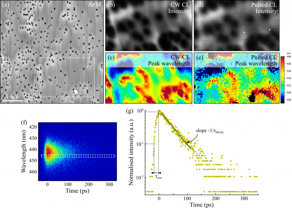
Carrier dynamics at trench defects in InGaN/GaN quantum wells revealed by time-resolved cathodoluminescence
Kusch et al., Nanoscale 14, 402 (2022)
DOI: 10.1039/D1NR06088K
Nanoscale 2022 Emerging Investigators
2021
Study of Ti contacts to corundum α-Ga2O3
Massabuau et al., J. Phys. D: Appl. Phys 54, 384001 (2021)
DOI: 10.1088/1361-6463/ac0d28
2021 Emerging Leaders
Progress in atomic layer deposited α-Ga2O3
materials and solar-blind detectors
Massabuau et al., Proc. SPIE 11687, 116870Q (2021)
DOI: 10.1117/12.2588729
Pure single-photon emission from an InGaN/GaN quantum dot
Holmes et al., APL Mater. 9, 061106 (2021)
DOI: 10.1063/5.0049488
Directly correlated microscopy of trench defects in InGaN quantum wells
O’Hanlon et al., Ultramicroscopy XXXX, 113255 (2021)
DOI: 10.1016/j.ultramic.2021.113255
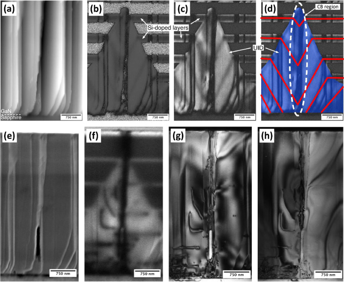
Dislocations at coalescence boundaries in heteroepitaxial GaN/sapphire studied after the epitaxial layer has completely coalesced
O’Hanlon et al., Ultramicroscopy XXXX, 113258 (2021)
DOI: 10.1016/j.ultramic.2021.113258
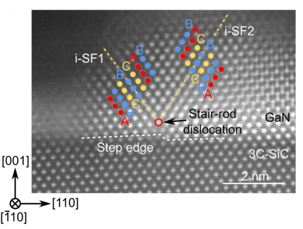
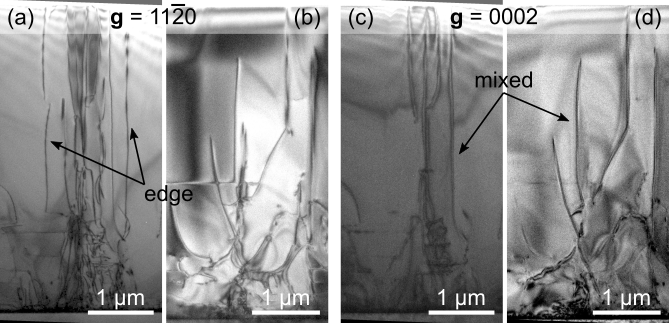
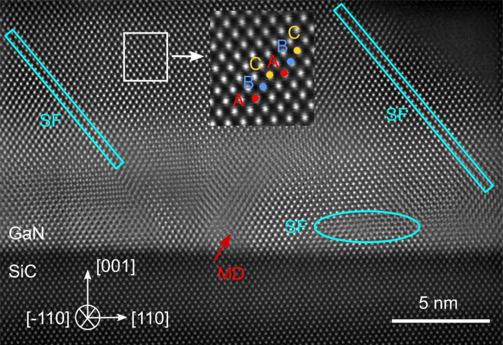
Defect structures in (001) zincblende GaN/3C-SiC nucleation layers
Vacek et al., J. Appl. Phys. 129, 155306 (2021)
DOI: 10.1063/5.0036366
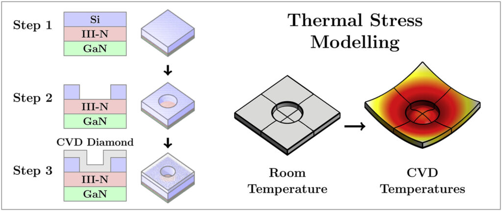
Thermal stress modelling of diamond on GaN/III-Nitride membranes
Cuenca et al., Carbon 174, 647 (2021)
DOI: 10.1016/j.carbon.2020.11.067
2020
Ti Alloyed α-Ga2O3: Route towards Wide Band Gap Engineering
Barthel et al., Micromachines 11, 1128 (2020)
DOI: 10.3390/mi11121128
Sequential plan-view imaging of sub-surface structures in the transmission electron microscope
Massabuau et al., Materialia 12, 100798 (2020)
DOI: 10.1016/j.mtla.2020.100798
Dislocations as channels for the etching of sub-surface porous GaN
Massabuau et al., APL Mater. 8, 031115 (2020)
DOI: 10.1063/1.5142491
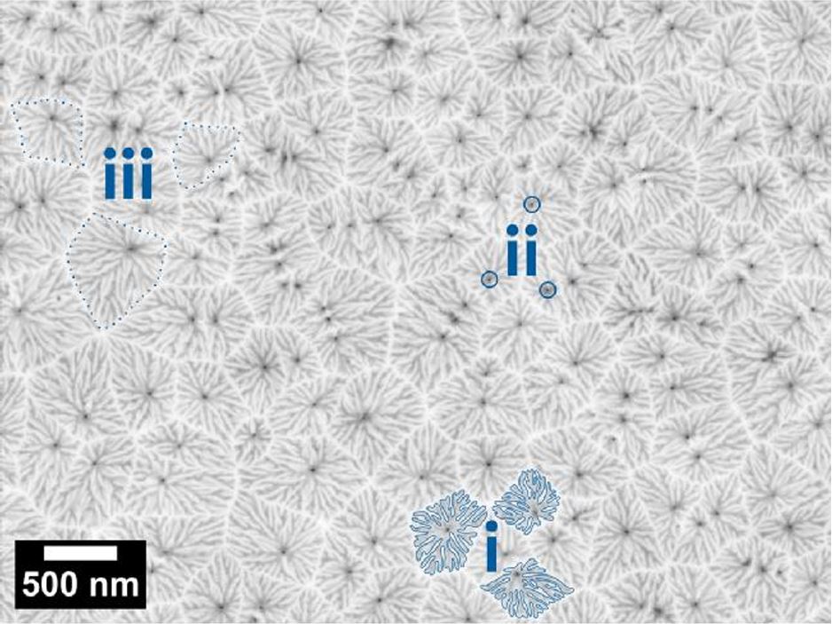
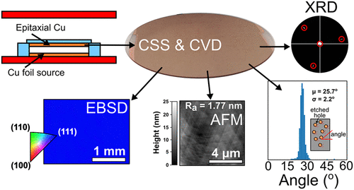
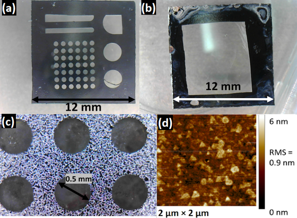
Integrated Wafer Scale Growth of Single Crystal Metal Films and High Quality Graphene
Burton et al., ACS Nano 14, 13593 (2020)
DOI: 10.1021/acsnano.0c05685
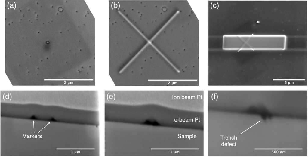
Cross-shaped markers for the preparation of site-specific transmission electron microscopy lamellae using focused ion beam techniques
O’Hanlon et al., Ultramicroscopy 212, 112970 (2020)
DOI: 10.1016/j.ultramic.2020.112970
Pair suppression caused by mosaic-twist defects in superconducting Sr2RuO4 thin-films prepared using pulsed laser deposition
Palomares Garcia et al., Commun. Mater. 1, 23 (2020)
DOI: 10.1038/s43246-020-0026-1
Mixed-size diamond seeding for low-thermal-barrier growth of CVD diamond onto GaN and AlN
Smith et al., Carbon 167, 620 (2020)
DOI: 10.1016/j.carbon.2020.05.050
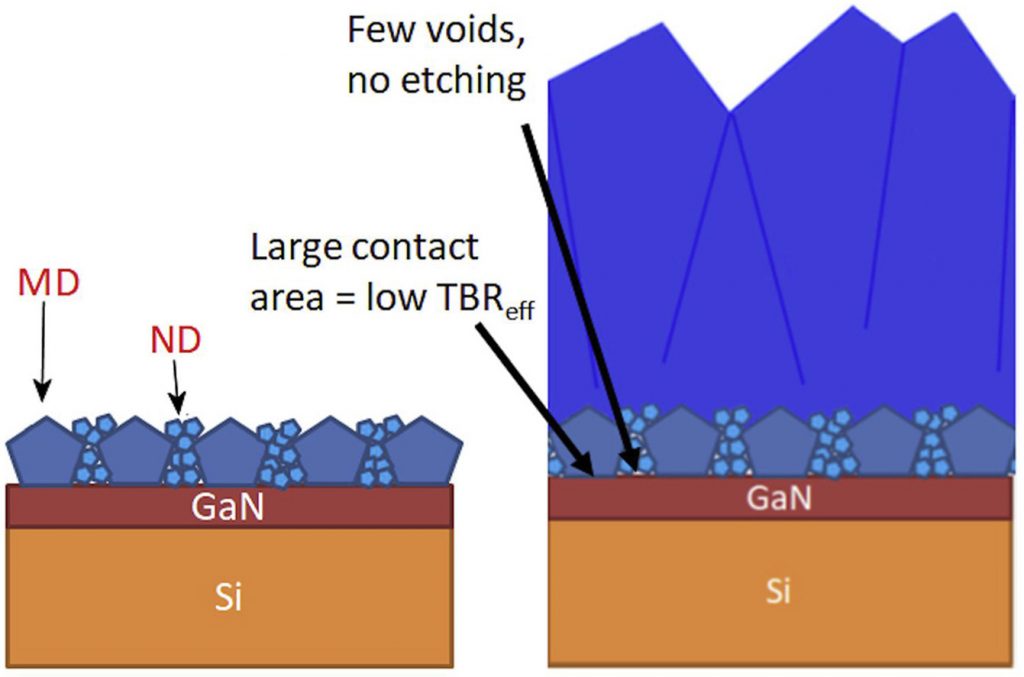
GaN-on-diamond technology platform: Bonding-free membrane manufacturing process
Smith et al., AIP Adv. 10, 035306 (2020)
DOI: 10.1063/1.5129229
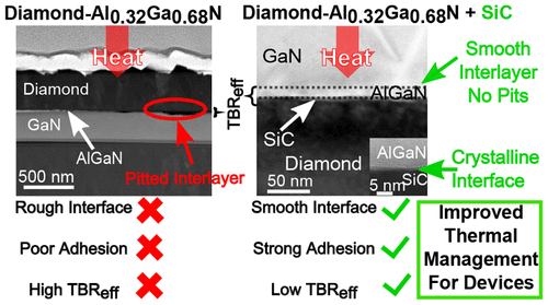
Crystalline Interlayers for Reducing the Effective Thermal Boundary Resistance in GaN-on-Diamond
Field et al., ACS Appl. Mater. Interfaces 12, 54138 (2020)
DOI: 10.1021/acsami.0c10129
2019
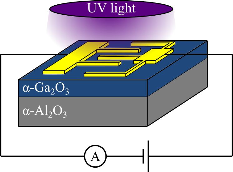
Atomic layer deposited α-Ga2O3 solar-blind photodetectors
Moloney et al., J. Phys. D: Appl. Phys. 52, 475101 (2019)
DOI: 10.1088/1361-6463/ab3b76
Low temperature growth and optical properties of α-Ga2O3 deposited on sapphire
by plasma enhanced atomic layer deposition
Roberts et al., J. Cryst. Growth 528, 125524 (2019)
DOI: 10.1016/j.jcrysgro.2019.125254
Optical and structural properties of dislocations in InGaN
Massabuau et al., J. Appl. Phys. 125, 165701 (2019)
DOI: 10.1063/1.5084330
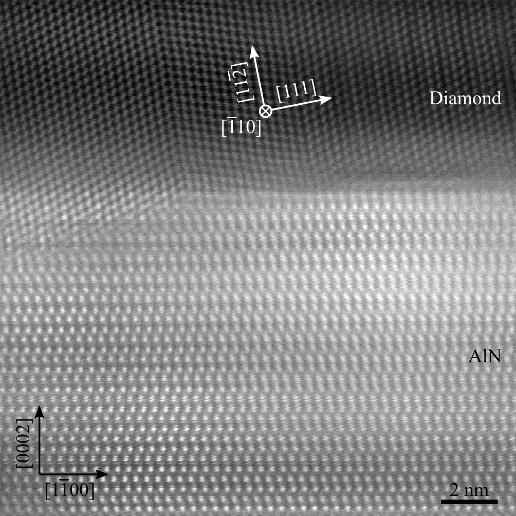
Thick adherent diamond films on
AlN with low thermal barrier resistance
Mandal et al., ACS Appl. Mater. Interfaces 11, 40826 (2019)
DOI:10.1021/acsami.9b13869
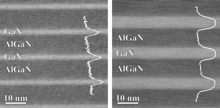
Impact of alloy fluctuations and Coulomb effects on the electronic and optical properties of c-plane GaN/AlGaN quantum wells
Roble et al., Sci. Rep. 9, 18862 (2019)
DOI: 10.1038/s41598-019-53693-2
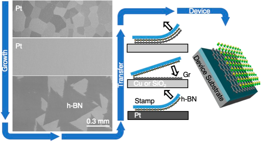
A Peeling Approach for Integrated Manufacturing of Large Monolayer h-BN Crystals
Wang et al., ACS Nano 13, 2114 (2019)
DOI: 10.1021/acsnano.8b08712
Effects of microstructure and growth conditions on quantum emitters in gallium nitride
Nguyen et al., APL Mater. 7, 081106 (2019)
DOI: 10.1063/1.5098794
Investigation of MOVPE-grown zincblende GaN nucleation layers on 3C-SiC/Si substrates
Lee et al., J. Cryst. Growth 524, 125167 (2019)
DOI: 10.1016/j.jcrysgro.2019.125167
2018
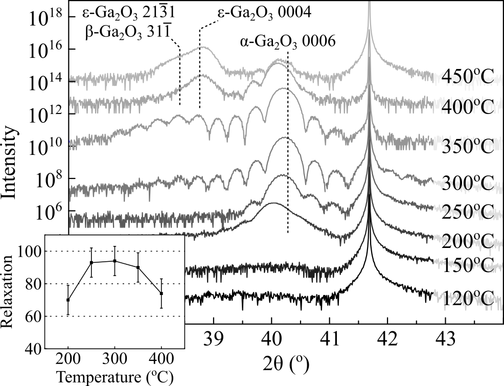
α-Ga2O3 grown by low temperature atomic layer deposition on sapphire
Roberts et al., J. Cryst. Growth 487 23 (2018)
DOI: 10.1016/j.jcrysgro.2018.02.014